What are you looking for?
Limited Time Offer on Signal Generators
Save 50% on all eligible bandwidth and performance options.
Unleash 800G / 1.6T Data Center Networking
Catch up on the latest innovations and challenges of 1.6T transceiver development with industry experts.
Save on Preconfigured DAQ Mainframes
Choose the multiplexer or switching bundle best suited for your application and save up to 10%.
Design, Emulation, and Test Solutions to Connect and Secure the World


See our latest innovations

UXM Wi-Fi 7 Wireless Emulation
The industry’s most comprehensive wireless emulator — now with turnkey Wi-Fi 7 MIMO signaling and throughput test.
MXG Signal Generator
Optimize signal generation for wideband multichannel applications.


EDA Software for RF Circuit Design
Simulate your 3DEM multi-technology designs up to 15 times faster.
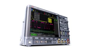

InfiniiVision 4000G X‑Series Oscilloscopes
Advance your R&D debug, serial test, and power analysis performance with our latest 7-in-1 instrument and embedded software.


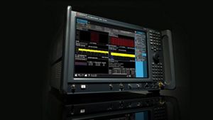
ENA-X Network Analyzer
Characterize power amplifier designs for 5G transmitters up to 50% faster with a single test setup.
Let our service be your strategic advantage
Empower your engineers to innovate boldly with strategic services across
the life cycle.
Automate intelligence with insights across your workflow


Find your solution
Test EV charging conformance
Emulate EV charging infrastructure to verify standard conformance.
Find your solution
Find your solution
Explore the next generation of technology innovation


Discover industry insights
Gain deep insights on emerging technologies and electronic design and test standards.


Learn with Keysight
Access e-learning for RF design, EDA, 5G, 6G, quantum computing, AV, EV, and test equipment.


Explore our events
Join us online or in person at conferences, trade shows, and webinars around the world.
Read our reviews
“Innovation in 5G technology is only possible when working side-by-side with partners like Keysight. Samsung has been at the forefront of 5G modem technology and with Keysight's emulators and test platforms, we are able to quickly develop and evaluate 5G NTN connections using our Exynos Modem development platform.”
Huiwon Je
Vice President, Modem Development Team
Samsung Electronics
Read our reviews
"We are delighted to have Keysight join the Intel Foundry Services EDA Alliance, enabling a range of RF simulation, design, and test capabilities from which IFS customers will benefit."
Rahul Goyal
Vice President, Product and Design Ecosystem Enablement
Intel
Read our reviews
“Our customers rely on our security solutions to protect them against threats. Keysight’s advanced test, visibility, and security will be welcomed by our customers looking for additional levels of protection.”
Rob Daniels
General Manager, Portfolio Strategy and Cybersecurity
BT Security
Read our reviews
“We were impressed with Keysight’s ability to thoroughly simulate real-world attack and traffic volume in the lab, helping us to identify and isolate issues quickly.”
Stuart Reid
Vice President of Engineering
Corsa Technology
Read our reviews
“Working with Keysight enabled us to meet the market demands on early creation and support for testing of NB-IoT devices with a powerful test solution for evaluating IoT device performance, which is particularly in challenging link budget conditions.”
Klas Arvidsson
Product Manager for OTA Solutions
Bluetest AB
Learn what's new at Keysight
Innovators start here
At Keysight, we empower innovators to explore, design, and bring world-changing technologies to life. Our software-centric solutions serve across the design and development environment, enabling you to deliver tomorrow’s breakthroughs at speed and with reduced risk.
Push the boundaries of engineering by quickly solving electronic design, network emulation, and test challenges to create the best product experiences. Improve your design and development process, optimize your network, and harness AI and digital twins to develop new solutions around 5G and 6G, EV and AV, IoT, and quantum computing. With Keysight at your side, forge ahead with confidence knowing your innovations will perform brilliantly in our connected and dynamic world.
Work with us
Keysight is always looking for people who share a passion for technology and innovation to join our team. At Keysight, you’ll work with the foremost experts in test and measurement science from around the world in a culture that embraces a bold vision of where technology can take us and a passion for tackling challenging problems with industry-first solutions.